


Overview
The CH32F203 is an industrial-grade enhanced low-power general-purpose MCU based on the Cortex-M3 core. CH32F203 features high performance. The system clock frequency can be up to 144MHz. Operating power consumption is as low as 69uA/MHz at the highest system clock frequency. CH32F203 integrates 2-channel USB interface which supports USB Host and USB Device functions, and provides abundant peripheral resources such as 1-channel CAN interface (2.0B active), 2 OPAs, 3 UARTs, 2 IIC interfaces, 12-bit ADC clock, and 10-channel Touchkey.
System Block Diagram
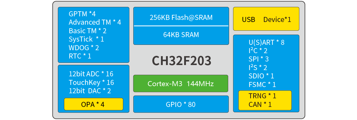
Features
- Cortex-M3 core, up to 144MHz system clock frequency.
- Single-cycle multiplication and hardware division.
- 20KB SRAM, 64KB Flash.
- Supply voltage: 2.5/3.3V. GPIO unit is supplied independently.
- Low-power modes: sleep, stop, standby.
- As low as 69.3uA/MHz in Run mode.
- As low as 22.4uA/MHz in Sleep mode.
- Power-on/power-down reset, programmable voltage detector.
- 2 x 18-channel general DMA.
- 2 operational amplifier comparators.
- 10-channel 12-bit ADC converters, 10-channel TouchKey.
- 4 timers.
- One USB2.0 full-speed host/device interface.
- One USB2.0 full-speed device interface.
- 3 USARTs.
- One CAN interface (2.0B active).
- 2 IIC interfaces, 2 SPI interfaces.
- 37 I/O ports, can be mapped to 16 external interrupts.
- CRC calculation unit, 96-bit unique ID.
- Serial 2-wire debug interface.
- Packages: LQFP48, LQFP32.
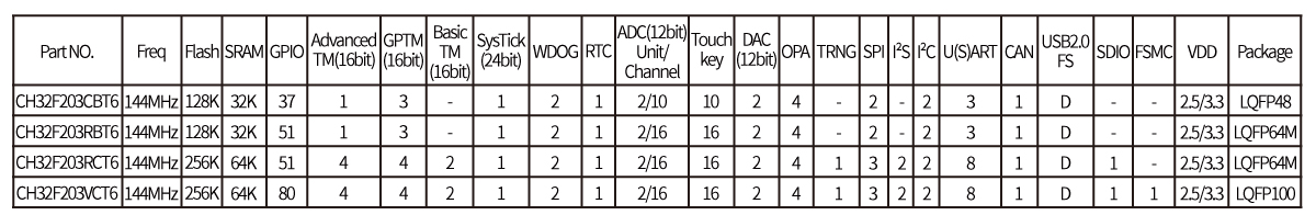
Product Selection Guide
Technical Resources
- Datasheet: CH32F20xDS0.PDF,CH32FV2x_V3xRM.PDF
- CH32F203EVT evaluation board manual and reference routines: CH32F20xEVT.ZIP